Have you ever wondered how the tiny chips in your smartphone or car navigate the world without failing? The answer lies in semiconductor cleanrooms—highly controlled environments where even a single speck of dust could sabotage an entire microchip. These spaces are the unsung heroes of modern technology, enabling everything from the latest AI-driven devices to life-saving medical equipment. But what exactly makes them so critical, and how do they work? Let’s dive in.
Understanding Semiconductors and Their Importance
What Are Semiconductors?
Semiconductors are materials—most commonly silicon—that conduct electricity partially, making them the backbone of electronic devices. Think of them as the bridge between insulators (like rubber) and conductors (like copper). Manufacturers transform pure silicon into thin wafers, which serve as the base for integrated circuits (ICs) or microchips. These chips are the brains behind every electronic device, from your coffee maker to fighter jets.
Why Are Semiconductors Sensitive to Contamination?
Here’s the catch: semiconductors are incredibly fragile. Even a single particle of dust (about 50 microns in size) can damage the nanoscale layers during chip fabrication. For context, a human hair is around 75 microns thick—so we’re talking about minuscule threats.
• Dust and Particles: Can cause short circuits or open circuits in the delicate circuitry.
• Static Electricity: A sudden discharge (ESD) can fry sensitive components, rendering chips useless.
• Humidity: Too much moisture leads to corrosion; too little creates static.
• Temperature Fluctuations: Even a 1°C change can warp wafers or alter chemical reactions during production.
In short, any contamination can lead to defective chips, wasted materials, and costly production delays. That’s where cleanrooms step in.
What Is a Semiconductor Cleanroom?
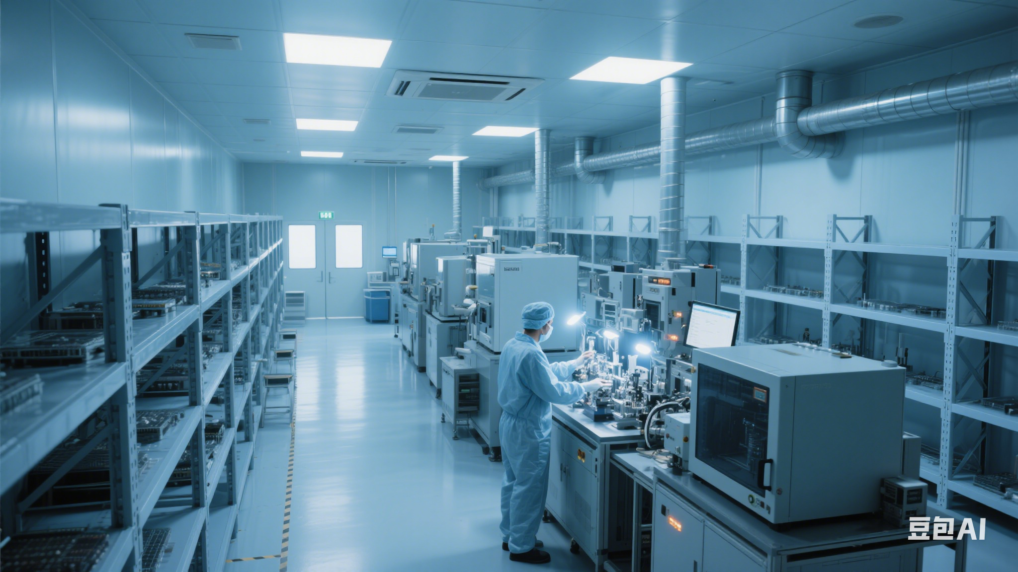
A semiconductor cleanroom is a sealed environment designed to eliminate contaminants and precisely control environmental factors. Unlike a typical “clean” room, these spaces are engineered to meet extreme standards:
• Purpose:
◦ Minimize airborne particles (dust, microbes, aerosol droplets).
◦ Maintain strict temperature (20–24°C ±1°C) and humidity (40–60% RH ±5%).
◦ Prevent static and electromagnetic interference.
◦ Ensure precision during processes like photolithography, etching, and deposition.
In other words, it’s a bubble where every molecule of air, every degree of temperature, and every static charge is monitored and managed.
How Semiconductor Cleanrooms Work
Air Filtration and Quality Control
The heart of any cleanroom is its air filtration system. Here’s how it keeps the air pristine:
HEPA and ULPA Filters
• HEPA (High-Efficiency Particulate Air): Removes 99.97% of particles ≥0.3 microns.
• ULPA (Ultra-Low Penetration Air): Goes a step further, trapping 99.9995% of particles ≥0.1 microns.Fun fact: A standard office has about 35 million particles per cubic meter (0.5 microns or larger). An ISO 5 cleanroom? Just 3,520 particles.
Airflow Systems
• Laminar Flow: Air moves in parallel, uniform layers (like a conveyor belt), minimizing turbulence and particle buildup. Used in critical areas like wafer handling.
• Turbulent Flow: Air circulates more freely, suitable for less sensitive zones (e.g., packaging).
ISO Standards
The International Organization for Standardization (ISO) classifies cleanrooms based on particle counts. For semiconductors:
• ISO 4–6: Used for fabrication (e.g., photolithography, etching).
• ISO 7–8: Suitable for testing, packaging, and assembly.
ISO Class | Particles ≤0.5μm per m³ | Common Use in Semiconductors |
ISO 4 | 352 | Extreme precision (e.g., EUV lithography) |
ISO 5 | 3,520 | Wafer processing |
ISO 6 | 35,200 | Deposition/etching |
ISO 7 | 352,000 | Testing |
Environmental Controls
Temperature Regulation
Why 20–24°C? Small fluctuations can cause thermal expansion or contraction of equipment and wafers, leading to alignment errors in chip patterns. Advanced HVAC systems use chilled water or glycol to maintain stability.
Humidity Control
Too dry = static buildup. Too wet = mold or corrosion. Cleanrooms use humidifiers/dehumidifiers to hit that 40–60% RH sweet spot, often with real-time sensors feeding data to centralized control systems.
ESD Prevention
Static is public enemy #1 in cleanrooms. Solutions include:
• Anti-static Flooring: Conductive materials (e.g., copper-infused tiles) that drain static to the ground.
• Ionizers:emit ions to neutralize static charges on surfaces and in the air.
• ESD- Safe Clothing: Coveralls, gloves, and shoe covers made from static-dissipative fabric.
Contamination Prevention Measures
Personnel Protocols
Humans shed skin cells, hair, and oils—all potential contaminants. Before entering, staff must:
• Wear full-body bunny suits (sterile, non-shedding coveralls).
• Use sticky mats to remove debris from shoes.
• Follow “no-touch” policies (e.g., using tweezers instead of fingers).
Material and Equipment Cleanliness
• Non-Shedding Surfaces: Walls and floors are made of stainless steel, epoxy, or vinyl—materials that don’t flake or absorb particles.
• Pre-Cleaned Equipment: All tools and machinery are washed with ultra-pure water (UPW) and ethanol before entering the cleanroom.
Chemical and Gas Handling
Certain processes (e.g., plasma etching) use toxic gases like sulfur hexafluoride (SF6). Cleanrooms have dedicated exhaust systems to remove fumes and prevent outgassing from equipment.
Semiconductor Cleanroom Classifications (ISO Standards)
The ISO 14644-1 standard is the gold standard for cleanroom classification. Here’s how it breaks down for semiconductors:
• ISO 3–5: Reserved for ultra-precision tasks like EUV (Extreme Ultraviolet) lithography, where chips are etched at the nanometer scale.
• ISO 6–8: Used for less sensitive steps, such as dicing wafers into individual chips or packaging them.
While ISO standards are universal, some industries add layers:
• Aerospace (NASA): Requires even stricter particle limits for chips in satellites or rockets.
• Automotive (ASTM): Focuses on reliability for chips in harsh environments (e.g., under the hood).
Key Applications of Semiconductor Cleanrooms
Microchip Fabrication
This is where the magic happens:
• Wafer Production: Pure silicon is melted, pulled into ingots, and sliced into wafers—all in ISO 5 cleanrooms.
• Photolithography: Light is used to imprint circuit patterns onto wafers. Even a single dust particle can blur the pattern, so this happens in ISO 4–5 environments.
• Etching and Deposition: Gases and plasmas carve or build layers on the wafer. These processes generate byproducts, so exhaust systems are critical.
Consumer Electronics
Your smartphone’s processor, laptop’s SSD, and smartwatch’s sensor all start in cleanrooms. For example:
• TSMC’s 5nm Chips: Used in iPhones, these require ISO 4 cleanrooms to handle the tiny transistor sizes (smaller than a virus!).
Automotive & Aerospace
• Self-Driving Cars: LiDAR sensors and AI chips need cleanrooms to prevent dust from interfering with precision optics.
• Spacecraft: Chips for satellites must withstand radiation and extreme temperatures, so cleanroom fabrication ensures no hidden defects.
Medical & Biotech
• Implantable Devices: Pacemakers and insulin pumps use microchips made in cleanrooms to prevent biological contamination.
• Diagnostic Tools: PCR machines and lab-on-a-chip devices rely on flawless chips for accurate results.
Design and Construction of Semiconductor Cleanrooms
Essential Design Features
Modular vs. Hardwall Cleanrooms
• Modular: Prefabricated panels installed on-site, ideal for quick setups or retrofits. Example: A startup might use a modular cleanroom for prototyping.
• Hardwall: Permanently built into the facility, with concrete or drywall. Used by giants like Intel for large-scale production.
Static-Dissipative Materials
• Flooring: Conductive vinyl or epoxy with copper mesh.
• Walls: Anodized aluminum or stainless steel, smooth to prevent particle buildup.
• Workbenches: Made of ESD-safe laminate or stainless steel, with built-in grounding straps.
Robotic Automation
To reduce human contact, many cleanrooms use:
• AMHS (Automated Material Handling Systems): Robotic arms that transport wafers between tools.
• Collaborative Robots (Cobots): Assist with assembly tasks while adhering to cleanroom standards.
Sub-Fab Considerations
Beneath the cleanroom lies the sub-fab—a hidden layer where utilities are managed:
• Ultra-Pure Water (UPW): Used to clean wafers, UPW is so pure it’s almost free of ions and organic matter.
• Gas Distribution: High-purity gases (e.g., nitrogen, argon) are piped in, while exhaust gases are filtered or scrubbed.
• HVAC Systems: Large air handlers with HEPA/ULPA filters cycle air through the cleanroom, often changing it 10–15 times per minute.
Safety is non-negotiable here:
• Fire Suppression: Inert gas systems (like FM200) to avoid water damage to equipment.
• Emergency Shut-offs: For gas and power in case of leaks or fires.
Challenges in Semiconductor Cleanroom Operations
Maintaining Ultra-Low Particle Counts
Even with filters, particles can sneak in via equipment or maintenance. Regular monitoring with particle counters and microbial samplers is essential.
Energy Consumption and Cost Efficiency
Cleanrooms are energy hogs:
• HVAC systems account for ~40% of a fab’s energy use.
• LED lighting and variable-speed fans can cut costs, but upfront investments are high.
Compliance with Evolving Standards
As chips get smaller (we’re now at 3nm and beyond), cleanroom requirements tighten. For example, EUV lithography demands ISO 3 conditions—10x cleaner than traditional ISO 5.
Handling Hazardous Materials
Chemicals like hydrofluoric acid (HF) and silane gas require strict safety protocols, including:
• Ventilated storage cabinets.
• Personal protective equipment (PPE) beyond standard bunny suits.
The Future of Semiconductor Cleanrooms
AI and IoT Integration
• Smart Monitoring: Sensors track particle counts, temperature, and equipment status in real time. AI algorithms predict maintenance needs (e.g., replacing a filter before it clogs).
• Automated Adjustments: If humidity spikes, IoT-enabled valves automatically adjust water flow in humidifiers.
Advanced Filtration
• Nanotechnology Filters: Being developed to trap even smaller particles (below 0.1 microns).
• Self-Cleaning Surfaces: Coatings that repel dust or break down organic contaminants via photocatalysis.
Automation and Robotics
• Fully Unmanned Cleanrooms: Companies like Samsung are testing fabs where robots handle 100% of production, eliminating human contamination risks.
• 3D Printing: Used to create custom fixtures or vents with smooth, particle-free surfaces.
Impact of Government Acts
• U.S. CHIPS and Science Act (2022): Allocates $52B for domestic semiconductor manufacturing, driving demand for new cleanrooms.
• European Chips Act: Aims to boost EU chip production to 20% of global output by 2030, requiring hundreds of new cleanrooms.
FAQs About Semiconductor Cleanrooms
Why Are Cleanrooms Necessary for Semiconductor Manufacturing?
Even a single particle can short-circuit a chip’s transistors, leading to product failures. Cleanrooms ensure that only controlled contaminants (if any) exist during production.
What’s the Difference Between ISO Class 5 and ISO Class 8 Cleanrooms?
• ISO 5: Allows 3,520 particles (0.5μm or smaller) per m³. Used for critical steps like photolithography.
• ISO 8: Allows 352,000 particles per m³. Suitable for packaging or quality control.
How Do Cleanrooms Prevent Static Damage?
Through a combo of anti-static flooring, ionizers, and ESD-safe materials. Even chairs and shelves are designed to dissipate static.
How Much Does a Semiconductor Cleanroom Cost?
• Modular (ISO 8): 50,000–200,000 for a small room (100–500 sq.ft.).
• Hardwall (ISO 5): 1M–10M+ for a large fab, depending on size, filters, and automation.
Can Existing Facilities Be Upgraded to Semiconductor-Grade Cleanrooms?
Yes, but it’s challenging. Retrofitting requires sealing gaps, installing new HVAC systems, and replacing materials with non-shedding alternatives. Modular cleanrooms are often the easiest upgrade path.
Need a Semiconductor Cleanroom Solution?
Whether you’re scaling production or launching a new chip design, partnering with cleanroom experts ensures your facility meets the highest standards. From modular setups to full-scale fabs, the right design can save costs, improve yields, and future-proof your operations.
Explore custom cleanroom solutions today to unlock the precision your semiconductor projects demand.
This article has integrated industry trends, technical standards, and real-world applications to provide a comprehensive guide to semiconductor cleanrooms. By prioritizing clarity and relevance, it aims to serve as a trusted resource for manufacturers, engineers, and tech enthusiasts alike.


